-
ULTRAFAST PHOTOVOLTAIC SPECTROMETER (UPVS)
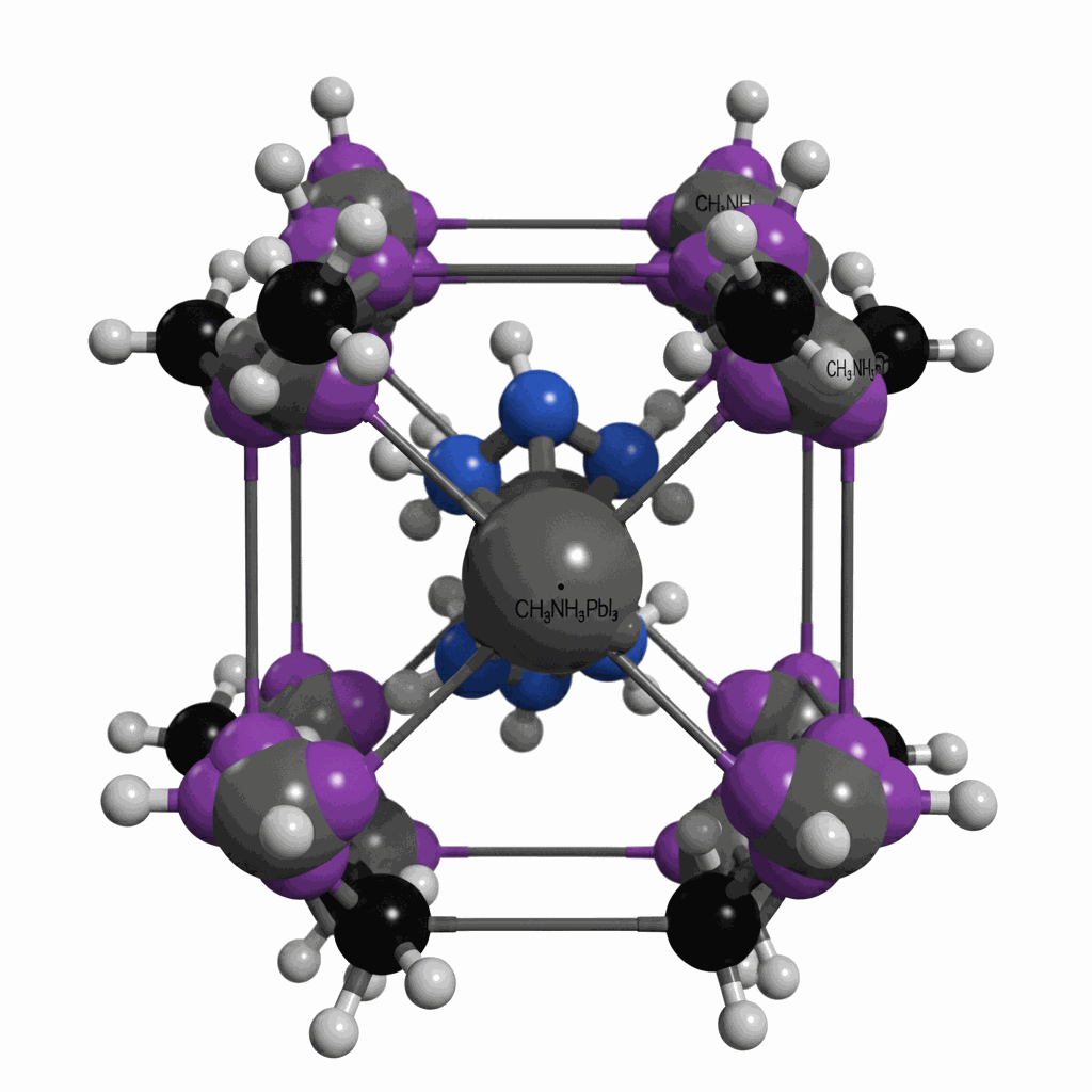
Perovskite Solar Cell
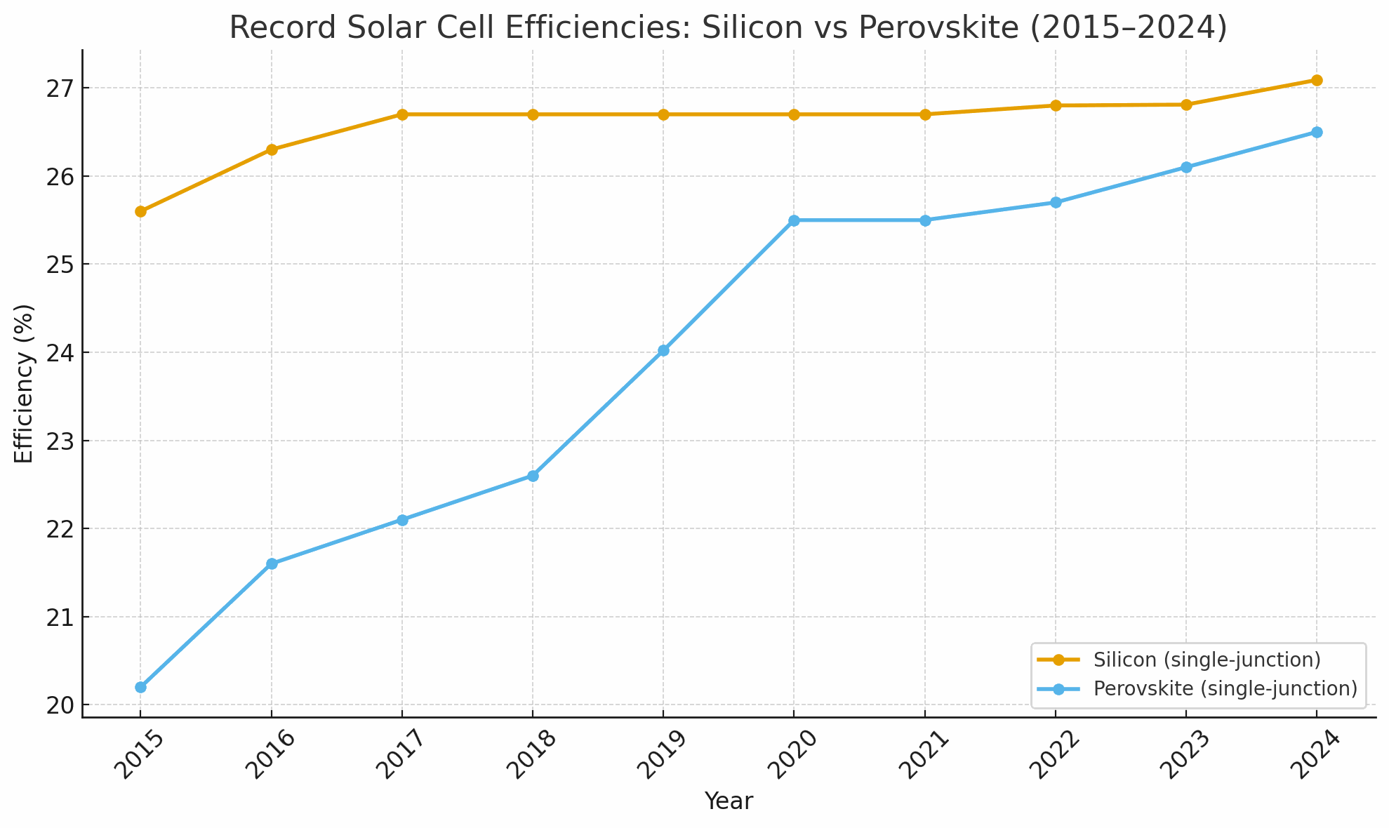
Perovskite solar cells are garnering significant interest as a potential solution to global energy challenges, primarily due to their exceptional efficiency and low cost. The core of their potential lies in the rapid progress they've made in converting sunlight into electricity, with laboratory efficiencies now rivaling and even surpassing that of traditional silicon solar panels. What makes this even more compelling is the simplicity of their manufacturing. Unlike silicon, which requires energy-intensive, high-temperature fabrication methods, perovskite cells can be produced using simple, solution-based processes like printing or spin-coating. This dramatically reduces the energy and cost of production. This unique combination of high performance and affordability positions them as a strong contender to revolutionize the renewable energy sector and accelerate our transition to a cleaner, more sustainable future..

Solving Fabrication Issues
A perovskite solar cell underperforms mainly because carriers get stuck or lost before reaching the electrodes. This happens due to defects/traps, fast recombination, hot carrier cooling, and poor interfaces. Even though perovskites have inherently great properties (high absorption, long diffusion lengths, high mobility), controlling defects and interfaces is the bottleneck for real-world efficiency.
Using Sciencetech UVPS
6 Steps to solve efficiency issues
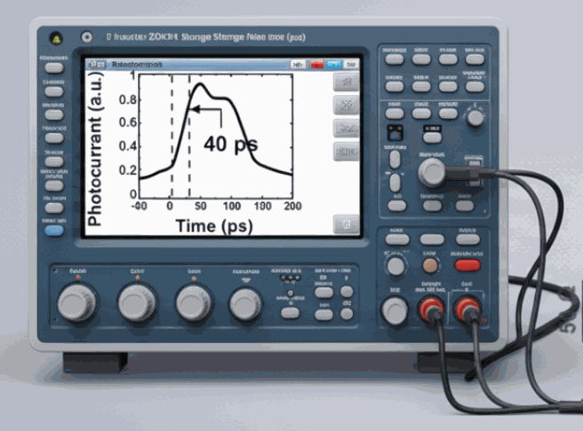
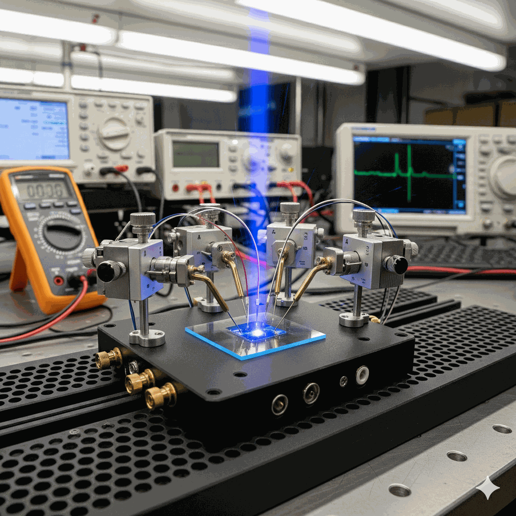
1) Device prep: Fabricate perovskite solar cell; integrate into a coplanar waveguide for <40 ps response.
2) Excitation: Illuminate via transparent contact with 400 nm femtosecond pulses at ~1-sun fluence.
3) Measurement: Record transient I–V under varied bias to capture ballistic (<200 ps), phonon-limited, and trap-assisted (>200 ps) regimes.
4) Temperature scan: Use Arrhenius analysis to extract trap energies and carrier lifetimes.
5) Analysis: Derive mobilities from field-dependent peak photocurrent.
6) Optimization: Modify grain size, passivate defects, tune ETL/HTL alignment; remeasure for higher Voc, mobility, and reduced trap effects
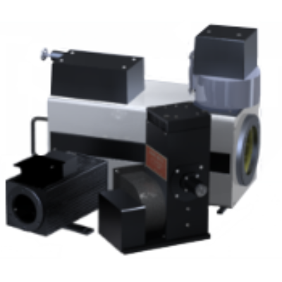
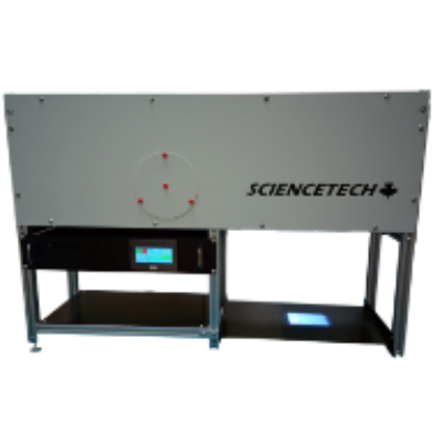
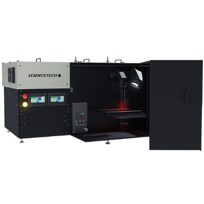
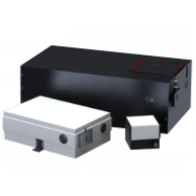
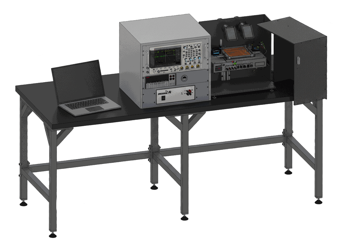
Sciencetech Turn Key Solution Ultrafast Photovoltaic Spectrometer
Key Specifications
|
|
Specification | ||||||
|
|
||||||
|
|
||||||
|
|
||||||
|
|
||||||
|
|
||||||
|
|
||||||
|
|
||||||
|
|
||||||
|
|
Sciencetech UPVS Excels at Testing
Perovskite solar cells
Single-junction 3D perovskites (e.g., MAPbI₃, FAPbI₃)
Mixed cation/anion perovskites
Perovskite tandems (with silicon, CIGS, organic, etc.)
2D layered perovskites
Organic photovoltaics (OPVs)
Single-junction OPVs
Tandem organic cells
Chalcogenide thin films
CIGS (Copper Indium Gallium Selenide)
CdTe (Cadmium Telluride)
Amorphous silicon (a-Si) thin-film solar cells
Quantum dot solar cells
PbS, PbSe, CsPbX₃ nanocrystals, etc.
Emerging materials
Lead-free perovskites (Sn-based, double perovskites like Cs₂AgBiBr₆)
Novel hybrid heterojunctions
Why Choose UPVS Over TRPL or TA?
Traditional optical methods like TRPL (time-resolved photoluminescence) and TA (transient absorption) provide insight into carrier lifetimes, but they measure light emission or absorption, not actual device current. In contrast, the Ultrafast Photovoltaic Spectrometer (UPVS) measures direct photocurrent in operating solar cells with sub-40 ps resolution. This means you capture real electrical behavior—carrier drift, trap dynamics, hot-carrier transport—exactly as they affect efficiency.
TRPL: Only sees radiative recombination; misses trap-assisted and non-radiative processes.
TA: Requires high pump fluences, probes optical signatures, not device-level current.
UPVS: Works at realistic 1-sun conditions, reveals true carrier mobility, extraction, and trap effects, directly tied to performance.
With UPVS, you’re not just observing photons—you’re measuring the electrons that matter for efficiency!
| Feature |
|
|
|
||||||||
|
|
Emitted photons from radiative recombination |
|
||||||||
|
|
> 100 ps |
|
||||||||
|
|
Optical-only, no direct link to current extraction |
|
||||||||
| Carrier processes captured |
|
|
|
||||||||
|
|
|
|
||||||||
|
|
No | No | ||||||||
|
|
|
|
||||||||
|
|
|
|
Unlike optical-only methods, UPVS reveals the true electrical heartbeat of a solar cell—capturing how charges move, get trapped, and are extracted—so you measure performance, not just photons.
Peer-Validated Performance

Nature Magazine
Leader in scientific journal and peer review

ACS Nano
Prominent Scientific Journel

Brock University
Cutting edge research in this feild
UPVS is not a prototype — it’s already trusted and published in the world’s leading journals. Multiple high-impact studies have relied on UPVS to uncover phenomena that traditional optical techniques could not. By choosing UPVS, you align your lab with cutting-edge researchers and a field-proven scientific method.
-
Nature Communications (2021): Directly resolved trap-assisted transport and shallow trap energetics with ps–ns precision.
-
ACS Nano (2023): Revealed band-like transport and phonon scattering before carrier trapping.
-
Follow-up publications (2023–2025): Demonstrated ballistic hot-carrier collection and quasi-3D free-carrier behavior in layered 2D perovskites.
Result: UPVS has already advanced the field — your lab can be next.
Software
Core Measurement Features
-
Automated time-resolved scans (ps → ns → ms range) with adjustable resolution.
-
Transient I–V mapping (bias-dependent dynamics plotted in real-time).
-
Temperature-dependent measurements with Arrhenius fitting for trap energy extraction.
-
Mobility extraction tools from field-dependent photocurrent (ϕ·μ calculation).
-
Hot-carrier analysis (transient Voc vs Eg tracking).
Automated time-resolved scans (ps → ns → ms range) with adjustable resolution.
Transient I–V mapping (bias-dependent dynamics plotted in real-time).
Temperature-dependent measurements with Arrhenius fitting for trap energy extraction.
Mobility extraction tools from field-dependent photocurrent (ϕ·μ calculation).
Hot-carrier analysis (transient Voc vs Eg tracking).
Data Handling & Analysis
-
Built-in fitting modules (exponential decays, trap-assisted tunneling, hopping models).
-
Spectral analysis tools when paired with tunable wavelength excitation.
-
Export to standard formats (CSV, MATLAB, Python, Origin, Igor).
-
Automated report generation (PDF/Word summary of key parameters).
Built-in fitting modules (exponential decays, trap-assisted tunneling, hopping models).
Spectral analysis tools when paired with tunable wavelength excitation.
Export to standard formats (CSV, MATLAB, Python, Origin, Igor).
Automated report generation (PDF/Word summary of key parameters).
User Interface & Workflow
-
Step-by-step measurement wizards for common experiments (lifetime, mobility, trap depth).
-
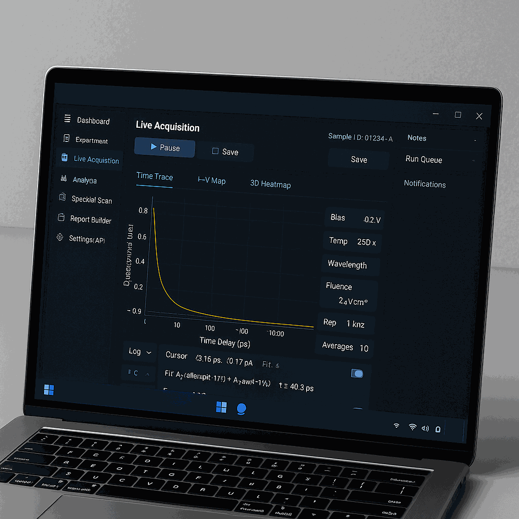
Live data visualization: oscilloscope-like transient traces, I–V overlays, 3D maps (time vs bias vs current).
-
Sample database: store measurement metadata (device type, fabrication notes, conditions).
-
Remote control/automation (LabVIEW, Python API, or REST interface for lab integration).
Step-by-step measurement wizards for common experiments (lifetime, mobility, trap depth).
Live data visualization: oscilloscope-like transient traces, I–V overlays, 3D maps (time vs bias vs current).
Sample database: store measurement metadata (device type, fabrication notes, conditions).
Remote control/automation (LabVIEW, Python API, or REST interface for lab integration).
Advanced Options (premium or future upgrades)
-
Machine learning fitting assistant (auto-selects decay model).
-
Batch analysis for multiple devices.
-
Simulation overlay (compare measured traces to drift-diffusion model predictions).
-
Alarm/flagging when traps, mobility, or lifetime fall below user thresholds.
Machine learning fitting assistant (auto-selects decay model).
Batch analysis for multiple devices.
Simulation overlay (compare measured traces to drift-diffusion model predictions).
Alarm/flagging when traps, mobility, or lifetime fall below user thresholds.
.